
Boundary Scan, also known as JTAG (Joint Test Action Group), is a technique used to test and debug chips without requiring physical access to their pins. It is based on the IEEE 1149.1–1990 standard, which defines a set of rules and protocols for chip communication. The core concept involves inserting a Boundary Scan Cell between each chip pin and its internal logic.
Why Boundary Scan?
When working with chips from different vendors that use various protocols and are assembled on a PCB, a unified way to test them together becomes essential. Boundary Scan provides this solution.
Purpose of Boundary Scan
- Fault Testing: Identifying faults in the interconnections between chips on a PCB.
- Internal Logic Access: Testing the internal logic of chips to verify functionality.
- Controllability & Observability: Controlling and observing the I/O pins of chips.
Components of JTAG
1. TAP (Test Access Port)
- Connects Chips to Tester: Allows external communication through JTAG signals.
- TAP FSM: A finite state machine managing test logic modes and operations.
- Five Pins:
- TCK: Test Clock.
- TMS: Test Mode Select.
- TDI: Test Data Input.
- TDO: Test Data Output.
- TRST: Test Reset (optional).
2. TAP Controller
- A finite state machine (FSM) with 16 states.
- Manages read/write operations via TDI and TDO pins.
3. Registers
- Instruction Register (IR): Stores instructions specifying operational modes and target data registers.
- Data Registers (DR): Stores data for testing. Types include:
- Boundary Scan Register (BSR): Observes and controls I/O pins.
- Bypass Register (BR): Bypasses chips during testing.
- ID Code Register: Stores chip ID information.
- Device-Specific Registers: Unique to the chip.
4. Instruction Decoder
- Decodes instructions from IR to control chip operations.
Boundary Scan Register (BSR)
- Purpose: Controls and observes I/O pins for testing.
- Operation: Managed via TAP controller for data transfer.
- Architecture: Boundary Scan Cells (BSCs) are arranged in a chain to cover all chip pins.
JTAG FSM States
- Test Logic Reset: Resets JTAG circuits.
- Run-Test/Idle: Initializes test logic.
- Select-DR/IR: Selects data or instruction registers.
- Capture-DR/IR: Captures data in registers.
- Shift-DR/IR: Serially shifts data in/out of registers.
- Update-DR/IR: Updates data from registers to system logic.
- Pause-DR/IR: Pauses data shifting temporarily.
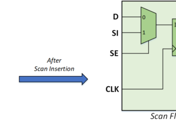
Boundary Scan Cell (BSC) Operations
- Capture Mode: Captures test responses from inputs.
- Shift Mode: Shifts data through the scan chain.
- Update Mode: Transfers data to output flops.
- Normal Mode: Acts as a transparent buffer connecting internal logic to I/O pins.
JTAG Instructions
- IDCODE: Retrieves the chip’s ID.
- BYPASS: Bypasses the chip, reducing test time.
- SAMPLE/PRELOAD: Captures or preloads pin values without interfering with logic.
- EXTEST: Tests interconnections between chips.
- INTEST: Tests internal chip functionality.
- HIGHZ: Isolates chip output pins (high-impedance state).
- CLAMP: Locks output pins to a specific value.
Summary
Boundary Scan / JTAG simplifies testing and debugging of chips on PCBs by providing standardized methods to control and observe chip operations. Its versatility, including fault detection, functionality verification, and reduced test times, makes it indispensable for modern electronic systems. By leveraging JTAG, engineers can ensure robust and efficient testing processes.